Feng3’s RCD Programmer is a very simple circuit that allows you to read and program low-pin-count PIC microcontrollers, using your PC’s RS-232 port. It also gets around the issue where some devices can’t be reliably reprogrammed by the official PICKit 3.
NOTE: Before you go and build this device, be aware that it may not work with RS-232 ports that put out less than ±7V. USB-to-RS232 adaptors, for example, often operate at only ±5V.
Rationale
I’ve been playing around with PIC microcontrollers, starting with Microchip’s simpler devices that have a low pin-count. I’ve chosen the PIC 12F629, with its 8 pins – up to 6 of which can be used for general-purpose I/O. In need of a way to read and write the flash program memory of the 12F629, I decided to build the very simple (but effective) RCD Programmer, designed by Feng3. It is controlled via a standard RS-232 port on your PC, using custom Windows software that drives the RS-232 lines directly.
Actually, building the RCD Programmer wasn’t my original plan. At first I bought a Sure Electronics clone of Microchip’s PICKit 3 programmer, and intended to just use that with MPLAB. However, I found out that the 12F629 (amongst others) has a certain mode that makes re-programming unreliable via the PICKit 3. When the PIC is configured to be completely free-running (i.e. internal oscillator, and internal-only reset), the only reliable way to bypass this state and enter programming mode is as follows:
- Start with VPP (pin 4 on 12F629), VDD (pin 1), and VSS (pin 8) all at GND.
- Raise VPP to VIHH (i.e. “programming voltage” – 13V assumed here, max. 13.5V).
- After at least 5μs, apply power (i.e. 5V) at VDD.
- After at least 5μs more, the device should be ready, in programming mode.
The programming specification (PDF) explains the “VPP before VDD” requirement, and yet the PICKit 3 is apparently unable to do this. The RCD Programmer, however, has been designed specifically for this purpose.
Schematics
Feng3’s original design is suitable for a variety of PIC ICs that can just be inserted bare, into a DIP socket. My requirements were a little different, because I’m working with a pre-made board that uses the 5-pin ICSP header – the same one used by the PICKit 3. Below you will see my version of the schematic for Feng3’s RCD Programmer:
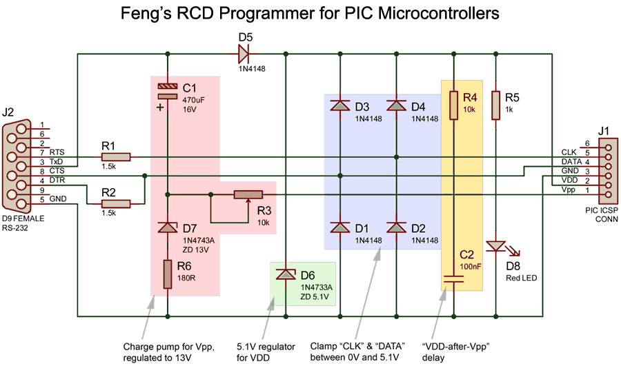 Figure 1: Schematic of Feng3's RCD Programmer for low-pin-count PIC microcontrollers
How it works
RS-232 Overview
The RCD Programmer is controlled via mis-use of the TxD, DTR, RTS, and CTS pins of an RS-232 port. That is to say, it is not at all using true RS-232 communications. Rather, software (Feng3’s PICProg4U) on the PC drives these lines (and reads the CTS input) directly.
The RS-232 standard defines that all signals are considered valid at ±3V → ±15V with respect to GND. The RCD Programmer will not operate properly at less than about ±7V – if your only RS-232 port is a USB-to-RS232 adaptor, you’re probably out of luck, since these may only operate at ±5V. My PC’s in-built COM1 port seems to output about ±9V and it works well, while my “HL-340” USB-to-RS232 adaptor does not.
In RS-232, TxD drives (and RxD receives) a negative voltage for a logic 1, and a positive voltage for logic 0. The other (control) signals use the opposite of this: positive means “active” and negative means “inactive”.
Signals used by the RCD Programmer
The RCD Programmer uses 4 of the RS-232 signals (plus GND) as follows:
- TxD (PC output): Used to charge C1 for VPP, then acts as power supply.
- RTS (PC output): Clock for PIC serial control.
- DTR (PC output): Drives the PIC data line for transmissions.
- CTS (PC input): This input will sense data from the PIC’s data line, when the PIC has been asked to transmit. In this case, R2 in the circuit allows for the PIC to override DTR.
Standard Operation
For simplicity, let’s assume your serial port outputs ±10V. Software on the PC controls (and reads) various lines of the RS-232 port directly, as follows:
Step 1: Charge C1
 Figure 2: Charging C1
TxD starts off asserted (i.e. -10V). Because it has a lower potential than GND, this allows current to flow forward through D7 to charge C1 (see Figure 2). The typical Zener voltage drop is about 0.65V so the initial current, , would be:
The capacitor should reach full charge within about seconds1:
Step 2: Raise VPP
 Figure 3: Vpp ready
Having allowed enough time for C1 to charge, TxD is inverted, raising it to +10V. At this point, C1’s charge was already at +10V. This adds to the voltage of TxD, for a total of +20V with respect to GND. This is a simple charge pump.
D7’s breakdown voltage of 13V will then act as a simple regulator to pull this +20V down to +13V, which provides the required “programming voltage” for the PIC. The 13V at the node between C1 and D7 is wired to the VPP pin of the PIC.
R3 (normally 10kΩ) is adjusted to allow sufficient current-flow to assert VPP, while ensuring C1 doesn’t discharge too quickly and drop out. The PIC needs at least (VDD+3.5) volts at VPP (i.e. at least 8.5V, since our PIC will be operated at VPP = 5V) for the entire duration of the programming-mode operation.
I’ve observed that usually the current at VPP is about 33μA, so we can estimate how long C1 will be able to keep VPP ≥ 8.5V
Step 3: Delay VDD
When TxD rises to +10V, not only does VPP rise to 13V, but then a sufficient forward voltage exists across D5. This would supply VDD, but is initially pulled down instead by the combination of R2 and C4. According to the datasheet (PDF), the 12F629 will start operating at somewhere around VDD ≥ 2.0V. We can calculate approximately when VDD will reach 2.0V as follows:
Stuff
puts 'This is some code in the Ruby language'